3D ICs Are Advanced Semiconductor Devices That Offer Improvements In Performance, Power Efficiency
 |
| 3D ICs |
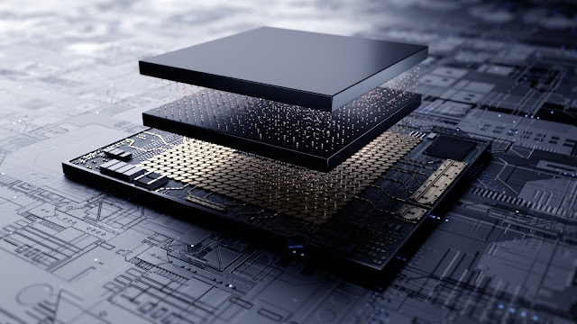
3D ICs (Three-Dimensional Integrated Circuits) are
advanced semiconductor devices that offer significant improvements in
performance, power efficiency, and form factor compared to traditional
two-dimensional integrated circuits. They are designed to overcome the
limitations of Moore's Law, which predicts the continuous miniaturization of
transistors on a single chip. By vertically stacking multiple layers of
circuitry, Three-Dimensional Integrated Circuits enable increased integration
of components, reducing interconnect lengths and improving overall system
performance. One of the key advantages of Three-Dimensional Integrated Circuits
is their ability to achieve higher transistor densities. Instead of spreading
transistors across a larger area, 3D IC stack them vertically, effectively
increasing the number of transistors per unit area. This dense integration
leads to faster and more powerful circuits, as signals need to travel shorter
distances, reducing latency and improving overall system speed.
According To Coherent Market
Insights, The 3D ICs Market Was Valued At
US$ 7,521.4 Mn In 2019 And Is Anticipated To Grow By 22.5% CAGR To US$ 38,252.9
Mn By 2027.
Furthermore,
3D ICs facilitate heterogeneous
integration, allowing different technologies and functionalities to be combined
in a single package. This enables the integration of processors, memory,
sensors, and other components on the same chip, leading to more efficient and compact
systems. For example, a 3D IC could incorporate a high-performance processor,
memory modules, and specialized accelerators, all interconnected within a small
footprint. Another advantage of 3D IC is their improved power efficiency. By
reducing interconnect lengths and parasitic capacitance, 3D IC can minimize
power consumption and improve signal integrity. The shorter interconnects also
help reduce signal delays and increase data transfer rates. This enhanced power
efficiency is crucial in modern electronic devices that demand both high
performance and long battery life.
The
manufacturing process for 3D ICs involves techniques such as through-silicon vias
(TSVs) and wafer bonding. TSVs are vertical interconnects that pass through the
silicon substrate, enabling electrical connections between different layers of
the 3D IC. Wafer bonding techniques are used to stack and bond the individual
layers together, ensuring proper alignment and electrical connectivity. Despite
their numerous advantages, there are also challenges associated with 3D IC. The
thermal management of stacked layers can be more complex compared to
traditional ICs due to heat dissipation issues. Additionally, the manufacturing
process for 3D IC is more intricate and expensive, requiring precise alignment
and control during the stacking and bonding steps. Nevertheless, the potential
benefits of 3D ICs have attracted
significant research and development efforts. They are being explored for
various applications, including high-performance computing, mobile devices,
networking equipment, and automotive electronics. The improved performance,
power efficiency, and compactness offered by 3D IC make them an attractive
option for addressing the ever-increasing demands of modern electronic systems.


Comments
Post a Comment